Sunday, 12 March 2017
Electrical Projects
http://nevonprojects.com/engineering-projects-2/electrical-engineering-projects/http://nevonprojects.com/engineering-projects-2/electrical-engineering-projects/
Saturday, 11 March 2017
The Lorentz forces and law
The Lorentz force

The flow of an electric current down a conducting wire is ultimately due to the motion of electrically charged particles (in most cases, electrons) through the conducting medium. It seems reasonable, therefore, that the force exerted on the wire when it is placed in a magnetic field is really the resultant of the forces exerted on these moving charges. Let us suppose that this is the case. Let $A$ be the (uniform) cross-sectional area of the wire, and let $n$ be the number density of mobile charges in the conductor. Suppose that the mobile charges each have charge $q$ and velocity ${\bf v}$. We must assume that the conductor also contains stationary charges, of charge $-q$ and number density $n$ (say), so that the net charge density in the wire is zero. In most conductors, the mobile charges are electrons and the stationary charges are atomic nuclei. The magnitude of the electric current flowing through the wire is simply the number of coulombs per second which flow past a given point. In one second, a mobile charge moves a distance $v$, so all of the charges contained in a cylinder of cross-sectional area $A$ and length $v$ flow past a given point. Thus, the magnitude of the current is $q n A v$. The direction of the current is the same as the direction of motion of the charges, so the vector current is ${\bf I}' = q nA {\bf v}$. According to Eq. (229), the force per unit length acting on the wire is \begin{displaymath} {\bf F} = q n A {\bf v}\times{\bf B}. \end{displaymath} (232) However, a unit length of the wire contains $nA$ moving charges. So, assuming that each charge is subject to an equal force from the magnetic field (we have no reason to suppose otherwise), the force acting on an individual charge is \begin{displaymath} {\bf f} = q {\bf v} \times{\bf B}. \end{displaymath} (233) We can combine this with Eq. (169) to give the force acting on a charge $q$ moving with velocity ${\bf v}$ in an electric field ${\bf E}$ and a magnetic field ${\bf B}$: \begin{displaymath} {\bf f} = q {\bf E} + q {\bf v} \times{\bf B}. \end{displaymath} (234) This is called the Lorentz force law, after the Dutch physicist Hendrik Antoon Lorentz who first formulated it. The electric force on a charged particle is parallel to the local electric field. The magnetic force, however, is perpendicular to both the local magnetic field and the particle's direction of motion. No magnetic force is exerted on a stationary charged particle. The equation of motion of a free particle of charge $q$ and mass $m$ moving in electric and magnetic fields is \begin{displaymath} m\frac{d{\bf v}}{dt} = q {\bf E} + q {\bf v} \times{\bf B}, \end{displaymath} (235) according to the Lorentz force law. This equation of motion was first verified in a famous experiment carried out by the Cambridge physicist J.J. Thompson in 1897. Thompson was investigating cathode rays, a then mysterious form of radiation emitted by a heated metal element held at a large negative voltage (i.e., a cathode) with respect to another metal element (i.e., an anode) in an evacuated tube. German physicists held that cathode rays were a form of electromagnetic radiation, whilst British and French physicists suspected that they were, in reality, a stream of charged particles. Thompson was able to demonstrate that the latter view was correct. In Thompson's experiment, the cathode rays passed though a region of ``crossed'' electric and magnetic fields (still in vacuum). The fields were perpendicular to the original trajectory of the rays, and were also mutually perpendicular. Let us analyze Thompson's experiment. Suppose that the rays are originally traveling in the $x$-direction, and are subject to a uniform electric field $E$ in the $z$-direction and a uniform magnetic field $B$ in the $-y$-direction. Let us assume, as Thompson did, that cathode rays are a stream of particles of mass $m$ and charge $q$. The equation of motion of the particles in the $z$-direction is \begin{displaymath} m \frac{d^2 z}{dt^2} = q\left(E - v B\right), \end{displaymath} (236) where $v$ is the velocity of the particles in the $x$-direction. Thompson started off his experiment by only turning on the electric field in his apparatus, and measuring the deflection $d$ of the ray in the $z$-direction after it had traveled a distance $l$ through the electric field. It is clear from the equation of motion that \begin{displaymath} d = \frac{q}{m} \frac{E t^2}{2} = \frac{q}{m} \frac{E l^2}{2 v^2}, \end{displaymath} (237) where the ``time of flight'' $t$ is replaced by $l/v$.

This formula is only valid if $d\ll l$, which is assumed to be the case. Next, Thompson turned on the magnetic field in his apparatus, and adjusted it so that the cathode ray was no longer deflected. The lack of deflection implies that the net force on the particles in the $z$-direction was zero. In other words, the electric and magnetic forces balanced exactly. It follows from Eq. (236) that with a properly adjusted magnetic field strength \begin{displaymath} v = \frac{E}{B}. \end{displaymath} (238) Thus, Eqs. (237) and (238) and can be combined and rearranged to give the charge to mass ratio of the particles in terms of measured quantities: \begin{displaymath} \frac{q}{m} = \frac{2 d E}{l^2 B^2}. \end{displaymath} (239) Using this method, Thompson inferred that cathode rays were made up of negatively charged particles (the sign of the charge is obvious from the direction of the deflection in the electric field) with a charge to mass ratio of $-1.7\times 10^{11}$ C/kg. A decade later, in 1908, the American Robert Millikan performed his famous ``oil drop'' experiment, and discovered that mobile electric charges are quantized in units of $-1.6\times 10^{-19}$ C. Assuming that mobile electric charges and the particles which make up cathode rays are one and the same thing, Thompson's and Millikan's experiments imply that the mass of these particles is $9.4\times 10^{-31}$ kg. Of course, this is the mass of an electron (the modern value is $9.1\times 10^{-31}$ kg), and $-1.6\times 10^{-19}$ C is the charge of an electron. Thus, cathode rays are, in fact, streams of electrons which are emitted from a heated cathode, and then accelerated because of the large voltage difference between the cathode and anode. Consider, now, a particle of mass $m$ and charge $q$ moving in a uniform magnetic field, ${\bf B} = B \hat{\bf z}$. According, to Eq. (235), the particle's equation of motion can be written: \begin{displaymath} m \frac{d{\bf v}}{dr} = q {\bf v}\times{\bf B}. \end{displaymath} (240) This reduces to $\displaystyle \frac{dv_x}{dt}$ $\textstyle =$ $\displaystyle {\mit\Omega} v_y,$ (241) $\displaystyle \frac{dv_y}{dt}$ $\textstyle =$ $\displaystyle -{\mit\Omega} v_x,$ (242) $\displaystyle \frac{d v_z}{dt}$ $\textstyle =$ $\displaystyle 0.$ (243) Here, ${\mit\Omega} = q B/m$ is called the cyclotron frequency. The above equations can be solved to give $\displaystyle v_x$ $\textstyle =$ $\displaystyle v_\perp \cos({\mit\Omega} t),$ (244) $\displaystyle v_y$ $\textstyle =$ $\displaystyle - v_\perp \sin({\mit\Omega} t),$ (245) $\displaystyle v_z$ $\textstyle =$ $\displaystyle v_\parallel,$ (246) and $\displaystyle x$ $\textstyle =$ $\displaystyle \frac{v_\perp}{\mit\Omega} \sin({\mit\Omega} t),$ (247) $\displaystyle y$ $\textstyle =$ $\displaystyle \frac{v_\perp}{\mit\Omega} \cos({\mit\Omega} t),$ (248) $\displaystyle z$ $\textstyle =$ $\displaystyle v_\parallel t.$ (249) According to these equations, the particle trajectory is a spiral whose axis is parallel to the magnetic field. The radius of the spiral is $\rho=v_\perp/{\mit\Omega}$, where $v_\perp$ is the particle's constant speed in the plane perpendicular to the magnetic field. The particle drifts parallel to the magnetic field at a constant velocity, $v_\parallel$. Finally, the particle gyrates in the plane perpendicular to the magnetic field at the cyclotron frequency. Finally, if a particle is subject to a force ${\bf f}$ and moves a distance $\delta {\bf r}$ in a time interval $\delta t$, then the work done on the particle by the force is \begin{displaymath} \delta W = {\bf f}\cdot \delta {\bf r}. \end{displaymath} (250) The power input to the particle from the force field is \begin{displaymath} P = \lim_{\delta t\rightarrow 0} \frac{\delta W}{\delta t} = {\bf f}\cdot {\bf v}, \end{displaymath} (251) where ${\bf v}$ is the particle's velocity. It follows from the Lorentz force law, Eq. (234), that the power input to a particle moving in electric and magnetic fields is \begin{displaymath} P = q {\bf v}\cdot {\bf E}. \end{displaymath} (252) Note that a charged particle can gain (or lose) energy from an electric field, but not from a magnetic field. This is because the magnetic force is always perpendicular to the particle's direction of motion, and, therefore, does no work on the particle [see Eq. (250)]. Thus, in particle accelerators, magnetic fields are often used to guide particle motion (e.g., in a circle) but the actual acceleration is performed by electric fields.

Monday, 6 March 2017
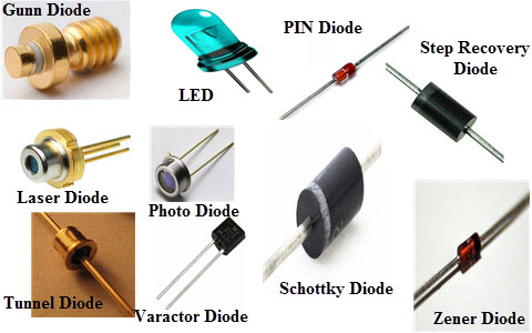
Different Types of Diodes and Their Uses
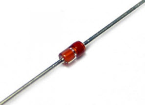
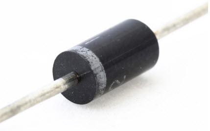
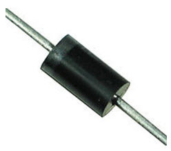
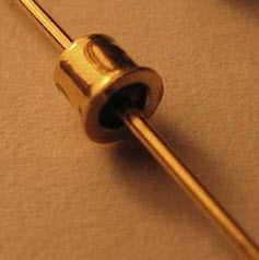
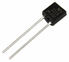
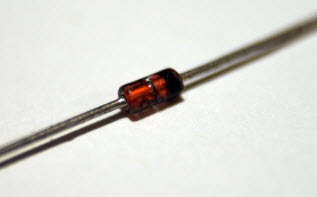
A diode is a two-terminal electrical device, that allows the transfer of current in only one direction.The diode is also known for their unidirectional current property, where the electric current is permitted to flow in one direction. Basically, a diode is used for rectifying waveforms, within radio detectors or within power supplies.They can also be used in various electrical and electronic circuits where ‘one-way’ result of the diode is required. Most of the diodes are made from semiconductors like Si (silicon), but sometimes, Ge (germanium) is also used.It is sometimes beneficial to summarize the different types of diodes are existing. Some of the types may overlap, but the various definitions may benefit to narrow the field down and offer an overview of the different diode types.
Different Types of Diodes
There are several types of diodes are available for use in electronics design, namely; a Backward diode, BARITT diode, Gunn Diode, Laser diode, Light emitting diodes, Photodiode, PIN diode, PN Junction, Schottky diodes, Step recovery diode, Tunnel diode, Varactor diode and a Zener diode.
Backward Diode
This type of diode is also called the back diode, and it is not widely used. The backward diode is a PN-junction diode that is similar to the tunnel diode in its process. It finds a few special applications where its specific properties can be used.
BARITT Diode
The short term of this diode Barrier Injection Transit Time diode is BARITT diode. It is applicable in microwave applications and allows many comparisons to the more widely used IMPATT diode. Please refer the below link for BARRITT Diode
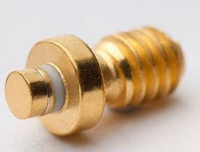
Gunn Diode
Gunn diode is a PN junction diode, this sort of diode is a semiconductor device that has two terminals. Generally, it is used for producing microwave signals. Please refer the below link for Gunn Diode Working, Characteristics, and its Applications
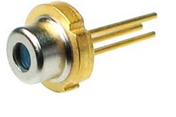
Laser Diode
The laser diode is not the similar as the ordinary LED (light emitting diode) because it generates coherent light. These diodes are extensively used in many applications like DVDs, CD drives and laser light pointers for PPTs. Although these diodes are inexpensive than other types of laser generator, they are much more expensive than LEDs. They also have a partial life.Please refer the below link for: for: How to Make a Laser Pointer
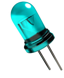
Light Emitting Diode
The term LED stands for light emitting diode, is one of the most standard types of the diode. When the diode is connected in forwarding bias, then the current flows through the junction and generates the light. There are also many new LED developments are changing they are LEDs and OLEDs.Please refer the below link for: LED light sources
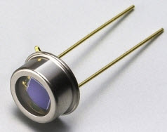
Photodiode
The photodiode is used to detect light. It is found that when light strikes a PN-junction it can create electrons and holes. Typically, photodiodes operate under reverse bias condition where even a small amount of flow of current resulting from the light can be simply noticed. These diodes can also be used to produce electricity.Please refer the below link for Photodiode Working Principle, and Its Characteristics
PIN Diode
This type of diode is characterized by its construction. It has the standard P-type & N-type regions, but the area between the two regions namely intrinsic semiconductor has no doping. The region of the intrinsic semiconductor has the effect of increasing the area of the depletion region which can be beneficial for switching applications.Please refer the below link for PIN Diode Basics, Working, and Its Applications.
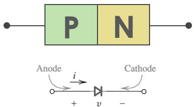
PN Junction Diode
The standard PN junction may be thought of as the normal or standard type of diode in use today. These diodes can come as small signal types for use in RF (radio frequency), or other low current applications which may be called as signal diodes. Other types may be planned for high voltage and high current applications and are normally named rectifier diodes.Please refer the below link for PN Junction Diode Theory and VI Characteristics
Schottky Diode
The Schottky diode has a lower forward voltage drop than ordinary Si PN-junction diodes. At low currents, the voltage drop may be between 0.15 & 0.4 volts as opposed to 0.6 volts for a Si diode. To attain this performance they are designed in a different way to compare with normal diodes having a metal to semiconductor contact. These diodes are extensively used in rectifier application, clamping diodes, and also in RF applications.Please refer the below link for Schottky Diode Working and Applications
Step Recovery Diode
A step recovery diode is a type of microwave diode used to generate pulses at very HF (high frequencies). These diodes depend on the diode which has a very fast turn-off characteristic for their operation.
Tunnel Diode
The tunnel diode is used for microwave applications where its performance surpassed that of other devices of the day.Please refer the below link for Tunnel Diode Circuit with Operation and Its Applications.
Varactor Diode or Varicap Diode
A varactor diode is one sort of semiconductor microwave solid-state device and it is used in where the variable capacitance is chosen which can be accomplished by controlling voltage. These diodes are also called as variceal diodes. Even though the o/p of the variable capacitance can be exhibited by the normal PN-junction diodes.But, this diode is chosen for giving the preferred capacitance changes as they are different types of diodes. These diodes are precisely designed and enhanced such that they allow a high range of changes in capacitance. Please refer the below link for Varactor Diode Working and Its Applications .
Zener Diode
The Zener diode is used to provide a stable reference voltage. As a result, it is used in vast amounts. It works under reverse bias condition and found that when a particular voltage is reached it breaks down. If the flow of current is limited by a resistor, it activates a stable voltage to be generated. This type of diode is widely used to offer a reference voltage in power supplies. Please refer the below link for Zener Diode Circuit Working and Its Applications.
Thus, this is all about different types of diodes and its uses.We hope that you have got a better understanding of this concept or to implement electrical projects please give your valuable suggestions by commenting in the comment section below. Here is a question for you, What is the function of a diode?
How To Use Transistor As A Switch
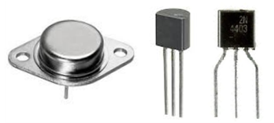
Types of BJT transistors
Basically, a transistor consists of two PN junctions, these junctions are formed by sandwiching either N-type or P-type semiconductor material between a pair of opposite type of semiconductor materials.
Bipolar junction transistors are classified into to types
- NPN
- PNP
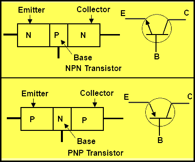
The transistor has three terminals, namely Base, Emitter, and Collector. The emitter is a heavily doped terminal and it emits the electrons into the Base region. The Base terminal is lightly doped and passes the emitter-injected electrons onto the collector. The collector terminal is intermediately doped and collects electrons from the Base.
An NPN type transistor is the composition of two N-type doped semiconductor materials between a P-type doped semiconductor layer as shown above. Similarly, A PNP-type transistors are the composition of two P-type doped semiconductor materials between an N-type doped semiconductor layer as shown above. The functioning of both NPN and PNP transistor is same but differ in terms of their biasing and power supply polarity.
Transistor As A Switch
If the circuit uses the BJT transistor as a switch, then the biasing of the transistor, either NPN or PNP is arranged to operate the transistor at the both sides of the I-V characteristics curves shown below. A transistor can be operated in three modes, active region, saturation region and cut-off region. In the active region, transistor works as an amplifier. The two operating regions of transistor Saturation Region (fully-ON) and the Cut-off Region (fully-OFF) were used to operate a transistor switch.
Operating Regions
We can observe from the above characteristics, the pink shaded area at the bottom of the curves represents the Cut-off region and the blue area to the left represent the Saturation region of the transistor. these transistor regions are defined as
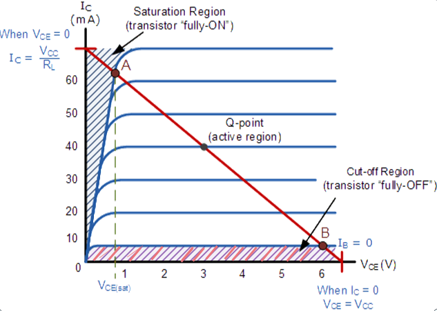
Cut-off Region
The operating conditions of the transistor are zero input base current (IB=0), zero output collector current(Ic=0), and maximum collector voltage (VCE) which results in a large depletion layer and no current flowing through the device. Therefore the transistor is switched to “Fully-OFF”. So we can define the cut-off region when using a bipolar transistor as a switch as being, bother the junctions of NPN transistors are reverse biased, VB< 0.7v and Ic=0. Similarly, for PNP transistor, the emitter potential must be –ve with respect to the base of the transistor.
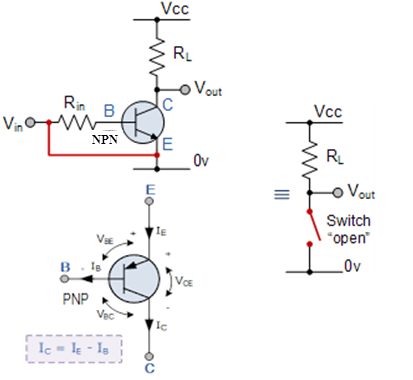
Then we can define the “cut-off region” or “OFF mode” when using a bipolar transistor as a switch as being, both junctions reverse biased, IC = 0 and VB < 0.7v. For a PNP transistor, the Emitter potential must be -ve with respect to the Base
Saturation Region
In this region, the transistor will be biased so that the maximum amount of base current(IB) is applied, resulting in maximum collector current(IC=VCC/RL) and then resulting in the minimum collector-emitter voltage(VCE ~ 0) drop. At this condition, the depletion layer becomes as small as the possible and maximum current flowing through the transistor. Therefore the transistor is switched “Fully-ON”.
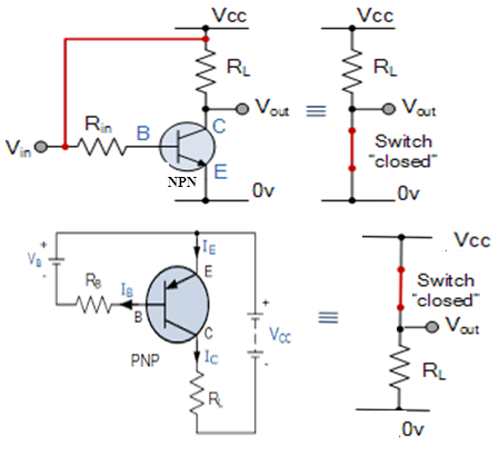
The definition of “saturation region” or “ON mode” when using a bipolar NPN transistor as a switch as being, both the junctions are forward biased, IC = Maximum and VB > 0.7v. For a PNP transistor, the Emitter potential must be +ve with respect to the Base.
Some of the basic Applications of Transistor as a Switch
In a transistor, unless a current flows in the base circuit, there is no current can flow in the collector circuit. This property will allow a transistor to be used as a switch. The transistor can be switched ON or OFF by changing the base. There are a few applications of switching circuits operated by transistors. Here, I considered NPN transistor to explain few applications which are using transistor switch.
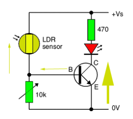
Light-Operated Switch
The circuit is designed by using a transistor as a switch, to light the bulb in a bright environment and to turn it off in the dark and a Light-Dependent Resistor (LDR) in the potential divider. When the environment dark LDR’s resistance become high. Then the transistor is switched OFF. When the LDR is exposed to the bright light, its resistance falls to less value resulting in more supply voltage and raising the base current of the transistor. Now the transistor is switched ON, the collector current flows and bulb lights up.
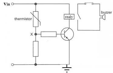
Heat-Operated Switch
One important component in the circuit of a heat-operated switch is the thermistor. The thermistor is a type of resistor that responds depending upon the surrounding temperature. Its resistance increases when the temperature is low and vice versa. When heat is applied to the thermistor, its resistance drops and the base current increases followed by a greater increase in the collector current and the siren will blow. This particular circuit is suitable as a fire alarm system.
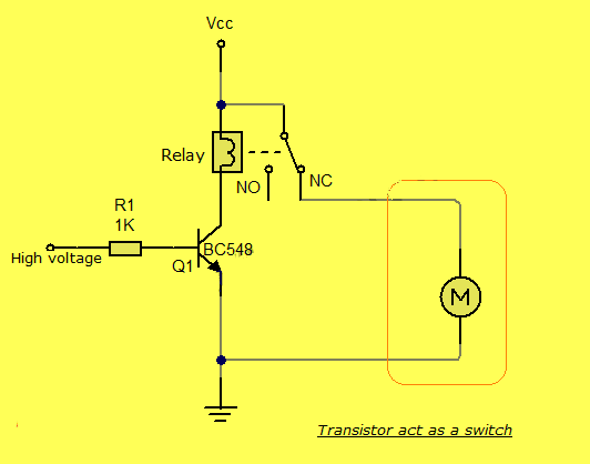
DC Motor Control (driver) in the Case of High Voltages
Consider no voltage is applied to the transistor, then the transistor becomes OFF and no current will flow through it. Hence the relay remains in OFF state. Power to the DC motor is fed from the Normally Closed (NC) terminal of the relay, so the motor will rotate when the relay is in OFF state. Apply of high voltage at the base of transistor BC548 causes turning ON of the transistor and the relay coil to energize.
Have you got the clear information of how a transistor can be used as a switch in different applications? We acknowledge that the above-given information clarifies the whole switching concept with related images and examples. Furthermore, any doubts regarding this concept or to implement any electrical projects, please give your suggestions and comments on this article you can write in the comment section below. Here is a question for you, What is the main function of a transistor?
Saturday, 18 February 2017
Saturday, 11 February 2017
solar energy definition ,& How We Make Solar Panels,also its discovery from root
DEFINATION:
IS DEVICE THAT CONVERT LIGHT ENERGY INTO ELECTRICAL ENERGY.

Crystal growing
SolarWorld heats and melts polysilicon rock until it forms a whitehot liquid, then re-fuses the molten silicon into a single giant crystal in which all atoms are perfectly aligned in a desired structure and orientation.
Charging
The magic starts with about 250 pounds of polysilicon rocks carefully stacked in a quartz crucible. The only other ingredient is a silicon disk impregnated with a tiny amount of boron. The addition of the oron dopant ensures that the resulting crystal will bear a positive potential electrical orientation. The crucible is encased within thick walls of insulating graphite and locked inside a cylindrical furnace.

Melting
As the crystal-growing furnace heats up to temperatures ranging around 2,500 degrees Fahrenheit, its silicon contents melt into a shimmering slurry. Once computerized monitors register the right temperature and atmospheric conditions, the alchemy begins. A silicon seed crystal, hung from a narrow cable attached to a rotary device atop the furnace, is slowly lowered into the melt.

Growing
The crucible starts to turn, and the seed crystal begins to rotate in the opposite direction. The silicon melt freezes onto the seed crystal, matching the seed’s crystalline structure. The crystal grows, the cable and seed slowly ascend, and the crystal elongates at a controlled width. As the growth depletes the silicon slurry, the crucible also rises.

Cooling
Flash forward about 2.5 days since the crucible was charged with polysilicon: After hours of cooling to about 300 degrees Fahrenheit, the furnace hood and shaft lift away from the crucible encasement, slowly swing to one side and reveal a completed cylindrical crystal, ready to move to the second step and next production room.
A silicon crystal must change shape several times before it winds up as the precisely calibrated wafers that form the foundations of photovoltaic cells.

Cutting
First, a saw cuts off the crystal’s so-called top and tail, so that a crystal of uniform width remains. Typically, wafering saws draw thin wire bearing a liquid abrasive across the crystal’s surface. (Below, a machine mounted with a giant donutlike steel blade does the cutting.) Wire saws also cut the crystal into ingots measuring 2 feet or less. Steel holders are mounted on the ends of these ingots for the next step.

Squaring
Mounted ingots are placed standing on end in a rack bearing 16 at a time inside another wireslicing machine. There, wire running in a lattice configuration descends on the ingots to shear off four rounded segments, leaving flat sides. The result: The ingots now have a square crosssection, except for still-rounded corners.

Slicing
The next wire saw is more intricate yet. A wire winding hundreds of times between two cylindrical drums forms a web of parallel, tightly spaced segments. As the wire unspools through the machine, ingots mounted sideways on glass and metal holders are pressed two at a time through the wire web, slicing them into the thickness of slim business cards. Each millimeter of crystal yields about 21/2 wafers. Detached from their holders, the wafers are loaded into carriers, or boats, for transport to the next step.
Converting wafers into cells
At this point, a wafer is no more capable of producing electricity than a sliver of river rock. The wafer is the main building block of a PV cell, but so far its only notable characteristics are its crystal structure and positive potential orientation. All of that changes in the third, multistep, cell-production phase of PV manufacturing.

Etching
In the only phase requiring a designated clean room, a series of intricate chemical and heat treatments converts the blank, grey wafers into productive, blue cells. A so-called texture etch, for instance, removes a tiny layer of silicon, relying on the underlying crystal structure to reveal an irregular pattern of pyramids. The surface of pyramids – so small they’re invisible to the naked eye – absorbs more light.
Diffusing
Next, wafers are moved in cartridges into long, cylindrical, ovenlike chambers in which phosphorus is diffused into a thin layer of the wafer surface. The molecular-level impregnation occurs as the wafer surface is exposed to phosphorus gas at a high heat, a step that gives the surface a negative potential electrical orientation. The combination of that layer and the boron-doped layer below creates a positive-negative, or P/N, junction – a critical partition in the functioning of a PV cell.

Coloring and Printing
The burgeoning, still-grey cells move in trays into heavy vacuum chambers where blue-purple silicon nitride is deposited onto their tops. The coating with silicon nitride – yet another member of the silicon family of materials – is designed to reduce reflection even further in the energy-dense blue end of the light spectrum. It leaves the cells with their final, dark color. Now, the cells can optimally gather photons and produce electricity. They lack, however, any mechanism to collect and forward the power. So, in a series of silkscreen- like steps, metals are printed on both sides of the cell, adding pin-stripe "fingers" and bus-bar circuitry. A functioning cell is born – only sunshine needed.
 Stringing cells into solar panels
Each phase of production depends on processes with flavors all their own. Careful control of heating and cooling dominates crystal growing. Wafering employs abrasion and cutting. Cell production concentrates on chemistry. Any factory process would be incomplete without a final assembly step, and in PV such a step is known as moduling.
Soldering
At SolarWorld, module manufacturing is a highly automated process, relying on robust steel robotics to undertake the increasingly heavy lifting of assembling lightweight PV cells into modules weighing around 45 pounds apiece. Each robotic tool works within a safety fence that, by design, excludes people. First, cells are soldered together into strings of 10, using an over-under-over-under pattern of metal connectors to link the cells. Six strings are laid out to form a rectangular matrix of 60 cells. Each matrix is laminated onto glass.
 Framing
To become a module, however, each laminate requires not only a frame to provide protection against weather and other impacts but also a junction box to enable connections among modules or with an inverter-bound conduit. Robots affix those, too.
 Inspection and Shipping
Careful cleaning and inspection provide final touches before each module can be palletized for delivery to homes and businesses.
Subscribe to:
Posts (Atom)

-
A diode is a two-terminal electrical device, that allows the transfer of current in only one direction.The diode is also known for their ...


